Dr. Valery Rudnev on . . .
Induction Hardening Tips: Equipment Selection for Scan Hardening, Part 2
This is the second installment of a multi-part column on equipment selection for induction heat treatment. Part 1, Dr. Valery Rudnev On . . . Induction Hardening Tips: Equipment Selection for Scan Hardening, covered types of scanners, scan hardening system setup, quenching challenges, maximizing process flexibility, and computer modeling. In this installment, Dr. Valery Rudnev discusses another critical aspect of induction scan hardening: inductor design subtleties and a comparison of different fabrication techniques (brazing vs. CNC
machining vs. 3D printing).
Introduction
Hardening inductors are often considered the weakest link in an induction hardening system because they may carry significant electrical power and operate in harsh environments exposed to high temperatures, water, and other coolants while being subjected to mechanical movement and potential sudden part contact.
Single-turn or multiturn inductors may be used in scan hardening (Figure 1). Copper profiling and the number of turns is determined by the workpiece geometry, required hardness pattern, and the ability to properly load match the coil to the power supply without reaching the operational limits or by other specific process requirements, such as the production rate or the hardness pattern runout/pattern cutoff. [1]

The longer (in case of horizontal arrangement) or the higher (vertical arrangement) the scan coil is, the faster the scan rate can be. This is due to the simple fact that the longer inductor leads to a longer period when the part will be inside the coil; therefore, the scan rate can be greater. However, limitations on the maximum length of the inductor’s heating face may be associated with the maximum permissible runout.
Hardness Pattern Runout Control
Single-turn inductors with narrow heating faces (3mm-6mm wide) are used where a sharp pattern runout is needed. An example of this would be the case where a pattern must end near a snap ring groove. Inductors with wider heating faces or two-turn coils can be used when a faster scan rate is desired and an extended runout is permitted. The main disadvantage to the excessively wide heating face is that it may result in an unspecified shift of coil current density when hardening complex geometric parts due to an electromagnetic proximity effect. [1]
Inductor Fabrication Techniques
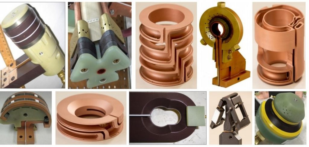
In applications where high process repeatability is critical (including automotive, aerospace, defense and other industries), the great majority of scan hardening inductors are CNC machined from a solid copper block, thus making them rigid, durable, and repeatable. CAD/CAM/CNC software programs are created that provide appropriate cutter-to-copper spatial relationships, which produce inductors of the required shape and precision regardless of complexity. Figure 2 shows a variety of finished and semi-finished CNC-machined hardening inductors. [2]

In other cases, copper tubing (square, rectangular, round, or die-formed shaped tubes) may be used for coil fabrication (Figure 3). Copper tubing is typically annealed to improve its ductility, bending properties, and workability. When sharp bends or complex coil shapes are required, inductor segments made from tubing are assembled by brazing. Joints are often overlapped, creating tongue-and-groove joints. Butt-joints should not be used.

A complex geometry inductor that contains numerous brazed joints, and elbow-type 90° joints in particular, could experience impeded water flow in the cooling coil turns, shortening coil life. Poor quality brazed joints are prime candidates for water leaks affecting not only the coil life expectancy but also a quality of hardened components due to a potential soft spotting in the areas of water leaks. Eliminating braze joints or dramatically reducing their number, particularly in current-carrying areas, is the key to fabricating durable, reliable, and long-last inductors.
Additive manufacturing (AM), or 3D printing, delivers successful fabrication of fixtures, tooling, holders, etc. Recently, some inductors have been fabricated using 3D printing as well. It is important to keep in mind that AM is not a single technology but it comprises a number of processes including direct metal laser sintering, electron beam melting, directed energy deposition, direct and indirect binder jetting, and others.
Depending upon a particular AM technique used in fabricating hardening inductors, it may face major challenges to match properties of pure copper. This includes (1) obtaining sufficiently high thermal conductivity (2) or low electrical resistivity, (3) ensuring high volumetric density, and (4) having minimum amount of residuals, just to name a few. All these factors affect coil life. Therefore, if you compare 3D printed inductors with brazed coils comprising numerous brazed joints, in the majority of cases, the life of 3D printed coils will surpass life of brazed inductors because of elimination of brazed joints in current-carrying regions. In addition, fabrication accuracy and repeatability of AM inductors typically surpasses the accuracy of brazed or bended coils.
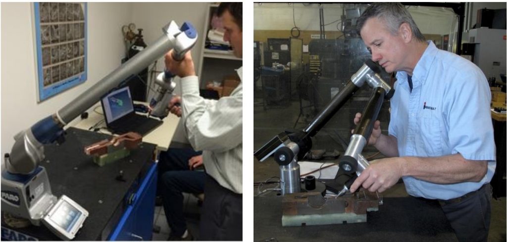
The situation is different when comparing life of 3D printed coils vs. CNC machined inductors. Fabrication accuracy of both processes is very similar, however, in high-power density applications even small degradation of above discussed four factors associated with AM might become essential causing greater probability of stress-fatigue and stress-corrosion copper failure of 3D printed coils compared to CNC machined inductors fabricated from pure copper. Another factor to consider is repairability of 3D printed inductors. If you need to do a revision then it would be most likely required you to re-manufacture 3D printed coils. Regardless of a fabrication method and for quality assurance purposes, it is beneficial to apply computerized 3D metrology laser scanner technology (Figure 4) to verify coil dimensional accuracy and alignment precision after inductor fabrication and assembly.

Material Selection
Copper and copper alloys are almost exclusively used to fabricate induction coils due to their reasonable cost, availability, and a unique combination of electrical, thermal, and mechanical properties. Proper selection of copper grade and its purity is crucial to minimize the deleterious effects of factors that contribute to premature coil failure including stress-corrosion and stress-fatigue cracking, galvanic corrosion, copper erosion, pitting, overheating, and work hardening. Cooling water pH also affects copper susceptibility to cracking.
Oxygen-free high-conductivity (OFHC) copper should be specified for most hardening inductors. In addition to superior electrical and thermal properties, OFHC copper dramatically reduces the risk of hydrogen embrittlement and developing localized “hot” and “cold” spots. The higher ductility of OFHC copper is also important because coil turns are subjected to flexing due to electromagnetic forces. The higher cost of OFHC copper is offset by improved life expectancy of hardening inductor.
For scan inductors that are intended to heat fillets, an appropriate copper heating face region must be focused into the fillet area. Coil copper profiling and the use of flux concentrators (flux intensifiers) are beneficial to focus the magnetic field into the fillet. These applications require careful design because the induced current has a tendency to take the shortest path and stay in the shaft area rather than flowing into the fillet [1]. Therefore, all efforts must be made to focus the heat generation into the fillet. Typically, higher frequencies work better for this purpose.
Copper Wall Thickness
It is important to maintain sufficient wall thickness to carry the electrical currents. The wall thickness of an inductor’s heating face should increase as frequency decreases. This fact is directly related to both the current penetration depth in the copper δCu. [1] It is highly desirable for the current-carrying copper wall thickness to be 1.6 times greater than the δCu calculated at maximum working temperature. Increased kilowatt losses in the copper, which are associated with reduced coil electrical efficiency and greater water-cooling requirements, will occur if the wall is thinner than 1.6∙δCu.
The table below shows the variation of δCu vs. frequency at room temperature (20°C/68°F).
In some cases, the copper wall thickness can be noticeably thicker than the recommended value of 1.6∙δCu. This is because it may be mechanically impractical to use a tubing wall thickness of, for example, 0.25 mm (0.01 in.).
I recommend Reference #1 to readers interested in further discussion on design of hardening inductors.
References
- V.Rudnev, D.Loveless, R.Cook, Handbook of Induction Heating, 2nd Edition, CRC Press, 2017.
- V.Rudnev, A.Goodwin, S.Phillip, W.West, S.St.Pierre, Keys to Long-lasting Hardening Inductors: Experience, Materials and Precision, Advanced Materials & Processes, October, 2015, p.48-52.
______________________________________________
Dr. Valery Rudnev, FASM, is the Director of Science & Technology, Inductoheat Inc., and a co-author of Handbook of Induction Heating (2nd ed.), along with Don Loveless and Raymond L. Cook. The Handbook of Induction Heating, 2nd ed., is published by CRC Press. For more information click here.


